
 Product
 Brand
Brand Articles
 Tools
Tools
What is an LDO (Low Dropout Regulator)?
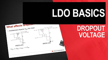
LDO basics: Dropout voltage
Topics covered in this article: |
Basics of LDO
LDO is a low dropout regulator, a kind of low dropout linear regulator. Traditional linear regulators, such as the 78XX series of chips require the input voltage to be at least 2V ~ 3V higher than the output voltage, otherwise, it will not work properly. But in some cases, such conditions are obviously too harsh, such as 5V to 3.3V. The voltage difference between the input and output is only 1.7v, which obviously does not meet the working conditions of traditional linear regulators. In response to this situation, chip manufacturers have developed the LDO class of voltage conversion chips.
LDO is a linear regulator that uses a transistor or field-effect transistor (FET) operating in its saturation region to produce a regulated output voltage by subtracting the excess voltage from the applied input voltage. The dropout voltage is the minimum difference between the input voltage and the output voltage required for the regulator to maintain the output voltage within 100mV above or below its rated value. LDO (low dropout) regulators with positive output voltage typically use a power transistor (also called a transfer device) as the PNP. This transistor allows saturation so the regulator can have a very low dropout voltage, typically around 200mV. By comparison, conventional linear regulators using NPN composite power transistors have a dropout of around 2V. A negative output LDO uses an NPN as its transfer device and operates in a similar mode to a PNP device for a positive output LDO.

LDO (Low Dropout Regulator)
If the input and output voltages are almost equal, it is best to use an LDO regulator that can achieve high efficiency. Therefore, LDO regulators are mostly used in applications where the lithium-ion battery voltage is converted to a 3V output voltage. Although the last ten percent of the battery's energy is not used, LDO regulators can still ensure that the battery's operating time is longer, while the noise is lower.
LDO usually has very low own noise and high power supply rejection ratio PSRR (Power Supply Rejection Ratio). Its biggest difference with the three-terminal regulator is that LDO is a very low self-consumption miniature system-on-chip (SoC). It can be used for current main channel control, integrated on-chip MOSFETs with very low in-line on-resistance, Schottky diodes, sampling resistors, and voltage divider resistors, and other hardware circuits, and has over-current protection, over-temperature protection, precision reference sources, differential amplifiers, delayers, etc. PG is a new generation of LDO, with each output state self-test, delayed safety power supply function.
Structure and Operating Principle of LDO
Structure
The structure of the LDO low dropout linear regulator mainly includes a start-up circuit, constant current source bias unit, enable circuit, adjustment element, reference source, error amplifier, a feedback resistor network, and protection circuit.
Operating Principle
The basic working principle of LDO is this: the system is powered up, if the enable pin is at a high level, the circuit starts. The constant current source circuit provides bias to the whole circuit, the reference source voltage is quickly established, the output rises continuously with the input. When the output is about to reach the specified value, the output feedback voltage obtained from the feedback network is also close to the reference voltage value. At this time the error amplifier will be the output feedback voltage and the reference voltage between the Error small signal for amplification and then amplified by the adjustment tube to the output, thus forming negative feedback, to ensure that the output voltage is stable at the specified value. The same, if the input voltage changes or output current changes, this closed-loop loop will keep the output voltage unchanged, that is: Vout = (R1 + R2)/R2 × Vref
As shown in the figure, the circuit consists of a series regulator VT, sampling resistors R1 and R2, and a comparison amplifier A.

The sample voltage is added to the inverting input of amplifier A, and compared with the reference voltage Uref added to the same phase input. The difference between the two is amplified by amplifier A, which controls the voltage drop of the series regulator, thus stabilizing the output voltage. When the output voltage Uout decreases, the difference between the reference voltage and the sampling voltage increases, the driving current at the output of the comparison amplifier increases, and the voltage drop of the series adjusting tube decreases, thus increasing the output voltage. On the contrary, if the output voltage Uout exceeds the desired setting value, the pre-drive current at the output of the comparison amplifier decreases, which results in a lower output voltage. The output voltage correction is performed continuously during supply, and the adjustment time is limited only by the response speed of the comparison amplifier and the output transistor circuit.
It should be noted that the actual linear regulator should also have many other features, such as load short circuit protection, overvoltage shutdown, overheat shutdown, reverse connection protection, etc., and the series regulator can also use MOSFETs.
Applications of LDO
The application of LDO is very simple, many LDO regulators only need to connect a capacitor at the input and output side to work stably. We need to consider important parameters such as differential voltage, quiescent current, PSRR, etc. in LDO application. In the system where the battery is used as the power supply, the LDO with the lowest possible differential voltage should be selected so that the battery can power the system for a longer time, such as NCP600, NCP629, etc.
Static current Iq is the abbreviation of Iquiescent, referring to the current consumed by the chip itself. Some engineers in the design of low-power systems, only consider the current consumed by the MCU itself but ignore the current consumed by the power supply chip, so that the standby power consumption of the whole system can not meet the standard. I have seen some engineers choose 78L05 to provide power for the MCU in the low-power system. After checking the datasheet, I can learn that the 78L05 Static current is 1mA, which is not suitable for low-power applications. We should choose NCP583 instead.
In RF, audio, ADC conversion, and other applications, PSRR (Power Supply Ripple Rejection Ratio) is a very important parameter, which reflects the noise immunity of the LDO. The higher the PSRR value the lower the LDO output ripple. The following lists some important characteristics and application directions of LDO.
Application areas of different voltage output levels
Voltage output level | Application areas |
1.25V | ARM9, FPGA, DSP, etc. |
1.8V | SDRAM, DDR RAM, etc. |
2.5V | MCU, DDR RAM, etc. |
3.0V | MCU, Nor Flash, Nand Flash, various other interface devices, etc. |
LDO characteristics and application direction
Characteristics | Application Direction |
Ultra-low ripple, high precision | Data acquisition |
Low differential voltage | Battery-powered |
Low quiescent current | Low power consumption applications, such as handheld meters |
Voltage monitoring | Embedded system power management |
Reset control | Industrial control |
Multi-channel output | Embedded systems that require multiple power supplies |
7 key points that must be mastered when designing an LDO
The traditional voltage regulator is obviously not suitable for the market, because, for some specific applications, the input and output voltage difference is too low to use. The LDO class power conversion chip was born to help us solve this problem well. However, here to remind everyone in the design of LDO should mainly consider the following issues.
1 Differential pressure (Uin-Uout) is an important parameter of the LDO, which indicates the potential difference between the input and output.
The smaller the differential pressure of the LDO, the better. But when the input voltage can not meet the "minimum differential pressure" requirements, the LDO can not work properly. At this time, the error amplifier will enter the full conduction state, so that the gain of the loop becomes zero, the regulating ability of the load will become very poor, and the power supply rejection ratio is also greatly reduced. The following points need to be noted.
First: In the LDO parameter table, it can have multiple or even multiple sets of differential voltage data, such as the minimum, typical and maximum values of differential voltage under light load, medium load, and full load conditions. Among them, the typical value is for design reference only. The most practical significance should be the maximum value of the differential pressure under full load conditions, which is measured under the most unfavorable conditions. The design should be based on this in order to allow enough margin to ensure that the LDO can work properly even under the worst conditions.
Second: For the sake of reliability, sometimes the minimum input voltage value can be selected according to the relation Uin=Uout+△U+lV. Power by 1.5 times more than the choice of a little waste (but add 20%-30% of the margin is not too much). General LDO self-loss power consumption is Pd_max = (Uin-Uout)*Iout.
Third: the input and output voltage difference is not a fixed value, it increases with the increase in output current and increases with the temperature.
2 Maximum output current. The maximum output current is a basic parameter of LDO.
Usually, the higher the output current, the higher the price of the LDO. The LDO must be able to provide sufficient current to the load under the most unfavorable operating conditions.
3 Input voltage requirements.
Input voltage must be greater than the rated output voltage and the sum of input an output voltage difference, that is, Uin>Uout + △ U. Otherwise, the LDO will lose the regulator function, the output voltage will change with the input voltage, then Uout is equal to the input voltage minus the product of adjusting tube on resistance (RON) and load current, that is, Uout = Uin - RONI0.
4 Output voltage fixed output LDO peripheral circuit is simple, easy to use.
It can save the cost of external sampling resistor divider and space. Its output voltage value has been converged at the factory (limited to the common voltage), and the output voltage accuracy is generally ±5%, which is sufficient for most applications. New LDO using laser correction technology, the accuracy index can reach ± 1% to ± 2%. Special attention needs to be paid to the conditions under which the accuracy specifications given in the product specification apply. Adjustable output LDOs allow the output voltage to be continuously adjusted within a specified range. If the output is connected to the feedback terminal so that the output voltage is equal to the internal reference voltage, the minimum output voltage is typically about 1.2V.
5 Input power supply types.
There are two types of input power supply, one is DC power supply and the other is AC power supply. When AC power is used, it should first be turned into pulsating DC power through the power transformer and rectifier filter, and then provide input voltage to the LDO. At this time, the differential voltage of the LDO is no longer a key indicator, because by increasing the number of turns of the secondary winding of the power transformer, it is easy to increase the input voltage of the LDO to meet the need of the LDO for differential voltage.
6 Quiescent current is the total current flowing to the ground inside the LDO under no-load conditions or when the output is turned off.
The lower the quiescent current, the lower the power consumption of the regulator. In some applications, standby mode is often selected to turn off the output, when the battery life depends on the size of the quiescent current. Recently introduced new LDO, the quiescent current can be as low as 75 to 150μA, and better than ordinary LDO voltage regulation characteristics. It should be emphasized that the quiescent current of LDO is not a fixed value, it increases with the increase of load current. However, the quiescent current of VLDO can be approximated as a constant value.
7 Additional functions of LDO
(1). The on/off control function allows a mechanical switch, gate circuit, or microcontroller to turn off the output of the LDO and put it into a low-power standby mode (also called standby mode).
(2). The input voltage reverse polarity protection function is used to prevent damage to the LDO when the input voltage polarity is reversed.
(3). Fault marker output function, when the output voltage (or input voltage) is lower than the specified threshold voltage, the LDO can output a fault marker signal. After receiving this signal, the microprocessor can complete the data storage and other work in time.
(4). Transient voltage protection function, the LDO will be used in automotive electronics, the need for transient changes in the load (such as sudden unloading) for protection. Once there is a transient voltage at the output, the output is immediately shut down. After the transient voltage has passed, and then quickly resumes normal operation.
(5). Tracking capability of some multi-output LDO needs to have tracking capability, where one or several auxiliary output voltages can automatically track changes in the main output voltage, and timely adjustment of their output voltage value, in order to reduce the relative change between the outputs.
(6). Sequencing, that is, in a power system consisting of multiple regulated power supplies, the output of each regulated power supply can be turned on or off in accordance with the specified order. In the design of LDO, if the above seven factors are taken into account, then you design the LDO is undoubtedly the best. Output ripple control can be achieved by improving the value of C61 to 220uf, 100uf, etc.
 UTMEL
UTMEL
We are the professional distributor of electronic components, providing a large variety of products to save you a lot of time, effort, and cost with our efficient self-customized service. careful order preparation fast delivery service
1.How much is the drop out voltage in LDO regulator?
The LDO regulator begins dropping out at 3.65-V input voltage; the range of the dropout region is between approximately 2-V and 3.65V input voltage.
2.How does a low drop out regulator work?
LDO is a linear voltage regulator that has a small voltage drop between the input and the output, and it works well even when the output voltage is very close to the input voltage unlike the linear voltage regulator that requires a large voltage drop between the input and the output to work properly.
 Discovering New and Advanced Methodology for Determining the Dynamic Characterization of Wide Bandgap DevicesSaumitra Jagdale15 March 20242674
For a long era, silicon has stood out as the primary material for fabricating electronic devices due to its affordability, moderate efficiency, and performance capabilities. Despite its widespread use, silicon faces several limitations that render it unsuitable for applications involving high power and elevated temperatures. As technological advancements continue and the industry demands enhanced efficiency from devices, these limitations become increasingly vivid. In the quest for electronic devices that are more potent, efficient, and compact, wide bandgap materials are emerging as a dominant player. Their superiority over silicon in crucial aspects such as efficiency, higher junction temperatures, power density, thinner drift regions, and faster switching speeds positions them as the preferred materials for the future of power electronics.
Read More A Comprehensive Guide to FPGA Development BoardsUTMEL11 September 202520577
This comprehensive guide will take you on a journey through the fascinating world of FPGA development boards. We’ll explore what they are, how they differ from microcontrollers, and most importantly, how to choose the perfect board for your needs. Whether you’re a seasoned engineer or a curious hobbyist, prepare to unlock new possibilities in hardware design and accelerate your projects. We’ll cover everything from budget-friendly options to specialized boards for image processing, delve into popular learning paths, and even provide insights into essential software like Vivado. By the end of this article, you’ll have a clear roadmap to navigate the FPGA landscape and make informed decisions for your next groundbreaking endeavor.
Read More 800G Optical Transceivers: The Guide for AI Data CentersUTMEL24 December 202510972
The complete guide to 800G Optical Transceiver standards (QSFP-DD vs. OSFP). Overcome supply shortages and scale your AI data center with Utmel Electronic.
Read More The 2026 Engineer’s Guide: Choosing the Right MCU for Your Next IoT & New Energy ProjectUTMEL30 April 2026908
A comprehensive comparison of 2026's leading MCUs from ST, NXP, and Microchip across power efficiency, processing performance, connectivity, and ecosystems to help engineers select the optimal chip for next-gen IoT and new energy projects.
Read More AI Server Components: Engineering Next-Gen Data Center Hardware for 100kW RacksUTMEL15 May 2026432
The transition from traditional enterprise IT to AI-driven workloads has rendered legacy data center hardware obsolete, forcing infrastructure planners to re-engineer server components for extreme thermal environments.
Read More
Subscribe to Utmel !
![MOC3010SM]() MOC3010SM
MOC3010SMON Semiconductor
![ADATE320-1KCPZ]() ADATE320-1KCPZ
ADATE320-1KCPZAnalog Devices Inc.
![AT88SC0104CA-SU]() AT88SC0104CA-SU
AT88SC0104CA-SUMicrochip Technology
![MOC3162M]() MOC3162M
MOC3162MON Semiconductor
![80HCPS1848CBLGI]() 80HCPS1848CBLGI
80HCPS1848CBLGIRenesas Electronics America Inc.
![HCS500-I/P]() HCS500-I/P
HCS500-I/PMicrochip Technology
![AD8190ACPZ-R7]() AD8190ACPZ-R7
AD8190ACPZ-R7Analog Devices Inc.
![ATA663231-GBQW]() ATA663231-GBQW
ATA663231-GBQWMicrochip Technology
![AD9942BBCZ]() AD9942BBCZ
AD9942BBCZAnalog Devices Inc.
![ATAES132A-SHEQ-B]() ATAES132A-SHEQ-B
ATAES132A-SHEQ-BMicrochip Technology


